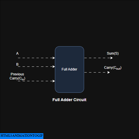
Full Adder circuit in Digital Logic
Full adder is a combinational circuit that adds two one-bit numbers and previous carry and then generates sum and carry as an output

4 steps that involved to construct any combinational circuit:
- Decide how many number of input lines and output lines required for the circuit.
- Construct the truth table according to number of input and output lines in which output as a function of input.
- Minimize the function using K-maps.
- Finally design the circuit by logical gates.
Step 1: Deciding number of input line and output lines for the Full-adder circuit:
Step2: constructing Truth Table for Full-Adder:
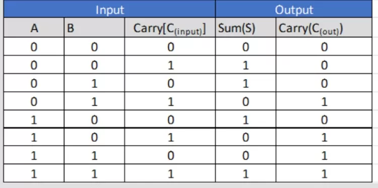
Step3: Now, you can construct k-map or you can write directly final boolean equation using min-terms of above truth table.

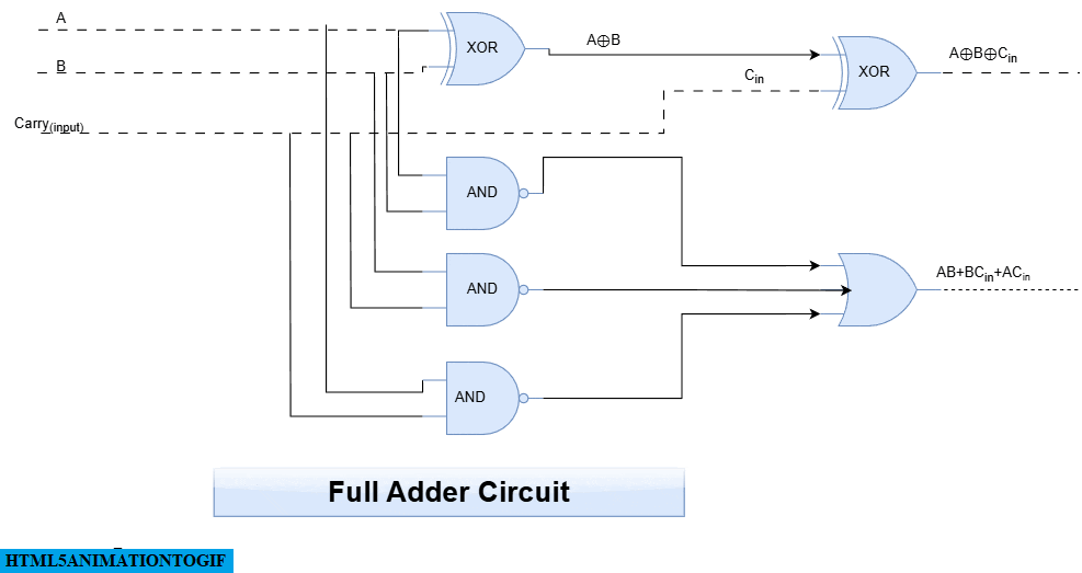
Step4: design the circuit by logical gates.
What's Your Reaction?